GND → Pins 4 and 5

If the keyboard consumes less than 100 mA, you can use a USB port as a power source.
If the keyboard consumes more power, you need a regulated 5 Volt DC adaptor or a USB charger to supply the power.
           +---+
        +--+   +--+
    +---+         +---+
    |                 |
    | | | | | | | | | |
    | | | | | | | | | |
    +-^-^-^-^-^-^-^-^-+
      1 2 3 4 5 6 7 8
Pin   Signal

1     Unused
2     Unused
3     TXD   (+)  (+ PWR)
4     RXD   (+)  (- PWR)
5     RXD   (-)  (- PWR)
6     TXD   (-)  (+ PWR)
7     Power (-)  (opt)
8     Power (+)  (opt)
 -----+ +--------------- 3
      | |
      ) (
      ) (
      ) *-- + PWR
      ) (
      ) (
      | |
 -----+ +--------------- 6

 -----+ +--------------- 4
      | |
      ) (
      ) (
      ) *-- - PWR
      ) (
      ) (
      | |
 -----+ +--------------- 5

 - PWR ----------------- 7


 + PWR ----------------- 8
The 7 - 8 pair is for an optional additional power supply.
Solder side;
         2                     2
    4    *    5           5    o    4
      *     *               o     o
   1 *       * 3         3 o       o 1

  180 degree Din Male    180 degree Din Female
Pin side;
         2                     2
    5    *    4           4    o    5
      *     *               o     o
   3 *       * 1         1 o       o 3
Midi uses a 180 degree 5 pin Din plug. The cable is a shielded twisted pair. The shield is connected to pin 2 (the top pin) at both ends of the cable. The cable uses male plugs at both ends. The female has pin 2 to ground at the sending side, not at the receiving side. This is done to avoid ground loops.
| 1 | Not Connected |
| 2 | GND |
| 3 | Not Connected |
| 4 | Midi |
| 5 | Midi |
Pin 4 of a female 180 degree Din plug is connected to + 5 Volt via a 220 Ω
resistor.
Pin 5 is connected via a 220 Ω resistor to;
+ 5 V for a logical 1
0 V for a logical 0
              +-----+
 + 5 V >------+ 220 +--> Din Pin 4
              +-----+

              +-----+
 Midi data >--+ 220 +--> Din Pin 5
              +-----+


 GND >-----------------> Din Pin 2
The LED part of an opto coupler is connected to pin 4 and 5 in series with a 220 Ω resistor;
                                       +5V
                                       \ /
                                        |
                                       +++
                                       | |
                                       +++
                                        |
              +-----+                   *---> Midi data
 Din Pin 4 >--+ 220 +---*-----+         |
              +-----+   |     |      | /
                      --+-- --+--    |/
                       /|\   \|/  -> |    Opto coupler
                      --+-- --+-- -> |\
                        |     |      |_\|
 Din Pin 5 >------------*-----+         |
                                        |
                                       \|/
                                       GND
This means that during a logical '0' a current of ca 5 mA runs through the cable. A disconnected cable signals a continuous '1', which means no data whatsoever.
This uses some of the pins of a game port.
        8 7 6 5 4 3 2 1
    -----------------------
     \  o o o o o o o o  /
       \ o o o o o o o /
         -------------
                   1
         5 4 3 2 1 0 9
| 1 | +5V |
| 4 | GND |
| 5 | GND |
| 8 | +5V |
| 9 | +5V |
| 12 | Midi TX |
| 15 | Midi RX |
There are 15 pins Sub-D to 2 x DIN adaptor cables for this port.
Some very old midi keyboards have a male 15 pin Sub-D connector.
        1 2 3 4 5 6 7 8
    -----------------------
     \  * * * * * * * *  /
       \ * * * * * * * /
         -------------
           1
         9 0 1 2 3 4 5
| 1 | +5V |
| 4 | GND |
| 5 | GND |
| 8 | +5V |
| 9 | +5V |
| 15 | Midi TX |
You can connect this with a male to female 15 pin Sub-D cable to an old
sound card.
Usually these keyboards also have a DIN connector you can use for MIDI. So
if your PC doesn't have a sound card with a 15 pins Sub-D connector, you
can connect this to a MIDI to USB adaptor instead.
However, some MIDI keyboards also get their power from this 15 pin Sub-D
connector. So if your PC doesn't have 15 pins Sub-D MIDI port, you need to
supply 5 Volt to this connector in order to power such a keyboard;
+5V → Pins 1, 8 and 9
GND → Pins 4 and 5
If the keyboard consumes less than 100 mA, you can use a USB port as a power
source.
If the keyboard consumes more power, you need a regulated 5 Volt DC
adaptor or a USB charger to supply the power.
              1
        3 2 1 0 9 8 7 6 5 4 3 2 1
    ---------------------------------
     \  o o o o o o o o o o o o o  /
       \ o o o o o o o o o o o o /
         -----------------------
                   2
         5 4 3 2 1 0 9 8 7 6 5 4

               DB-25 Female
 1    Shield
 2    Transmitted Data (A)
 3    Received Data (A)
 4    Request To Send (A)
 5    Clear To Send (A)
 6    DCE Ready (A)
 7    Gnd
 8    Received Line Signal Detector (A)
 9    Receiver Signal Element Timing (B)
10    Received Line Signal Detector (B)
11    Ext. Transmit Signal Element Timing (B)
12    Transmit Signal Element Timing (B)
13    Clear To Send (B)

14    Transmitted Data (B)
15    Transmit Signal Element Timing (A)
16    Received Data (B)
17    Receiver Signal Element Timing (A)
18    Local Loopback
19    Request To Send (B)
20    DTE Ready (A)
21    Remote Loopback
22    DCE Ready (B)
23    DTE Ready (B)
24    Ext. Transmit Element Timing (A)
25    Test Mode
        1 2 3 4 5
    -----------------
     \  * * * * *  /
       \ * * * * /
         -------
         6 7 8 9

        DE-9 Male
| 1 | DCD | Data Carrier Detect |
| 2 | RXD | Received Data |
| 3 | TXD | Transmitted Data |
| 4 | DTR | Data Terminal Ready |
| 5 | GND | GrouND |
| 6 | DSR | Data Set Ready |
| 7 | RTS | Request To Send |
| 8 | CTS | Clear To Send |
| 9 | RI | Ring Indicator |
Note: RTS is also known as RTR, Ready To Receive.
                          1
        1 2 3 4 5 6 7 8 9 0 1 2 3
    ---------------------------------
     \  * * * * * * * * * * * * *  /
       \ * * * * * * * * * * * * /
         -----------------------
                     2
         4 5 6 7 8 9 0 1 2 3 4 5

                DB-25 Male
 1
 2    TXD               Transmitted Data
 3    RXD               Received Data
 4    RTS               Request To Send
 5    CTS               Clear To Send
 6    DSR               Data Set Ready
 7    GND               GrouND
 8    DCD               Data Carrier Detect
 9    TEST
10    TEST
11    STF               Select Transmit Frequency
12    SDCD              Secondary DCD
13    SCTS              Secondary CTS

14    STXD              Secondary TXD
15    TXC               DCE TX Clock
16    SRXD              Secondary RXD
17    RXC               RX Clock
18
19    SRTS              Secondary RTS
20    DTR               Data Terminal Ready
21    SQ                Signal Quality
22    RI                Ring Indicator
23    CH/CI             rate select
24    XTC               DTE TX Clock
25
Note: RTS is also known as RTR, Ready To Receive.
Note: Pin 1 used to be protective ground.
The shield should be connected (soldered) to the connector shell at both
ends of the cable.
                 ACEHKM
      ACEHKMPSUWYACEHKM

     -------------------
    |  * * * * * * * *  |
    | * * * * * * * * * |
    |  * * * * * * * *  |
    | * * * * * * * * * |
     -------------------
                 BDFJLN
      BDFJLNRTVXZBDFJLN
 A    Chassis Ground
 B    Signal Ground
 C    Request To Send
 D    Clear To Send
 E    Data Set Ready
 F    Data Carrier Detect
 H    Data Terminal Ready
 J    Ring Indicator
 K
 L
 M
 N
 P    Transmitted Data (A)
 R    Received Data (A)
 S    Transmitted Data (B)
 T    Received Data (B)
 U    Terminal Timing (A)
 V    Receive Timing (A)
 W    Terminal Timing (B)
 X    Receive Timing (B)
 Y    Transmit Timing (A)
 Z
AA    Transmit Timing (B)
BB
CC
DD
EE
FF
HH
JJ
KK
LL
MM
NN
V35 used to be modem standard; A 48 kbps data signal was ASK modulated on a 60 kHz carrier, the lower sideband suppressed, resulting in a 60 ... 108 kHz bandwidth. Somehow V35 is now used as a name for this connecter.
                          1
        9 8 7 6 5 4 3 2 1 0 9 8 7 6 5 4 3 2 1
    ---------------------------------------------
     \  o o o o o o o o o o o o o o o o o o o  /
       \ o o o o o o o o o o o o o o o o o o /
         -----------------------------------
                       3                   2
         7 6 5 4 3 2 1 0 9 8 7 6 5 5 3 2 1 0

                        DC-37
 1    Shield
 2    Signal Rate Indicator
 3
 4    Send Data (A)
 5    Send Timing (A)
 6    Receive Data (A)
 7    Request To Send (A)
 8    Receive Timing (A)
 9    Clear To Send (A)
10    Local Loopback
11    Data Mode (A)
12    Terminal Ready (A)
13    Receiver Ready (A)
14    Remote Loopback
15    Incoming Call
16    Select Frequency
17    Terminal Timing (A)
18    Test Mode
19    Signal Ground

20    Receive Common
21
22    Send Data (B)
23    Send Timing (B)
24    Received Data (B)
25    Request To Send (B)
26    Receive Timing (B)
27    Clear To Send (B)
28    Terminal In Service
29    Data Mode (B)
30    Terminal Ready (B)
31    Receiver Ready (B)
32    Select Standby
33    Signal Quality
34    New Signal
35    Terminal Timing (B)
36    Standby Indicator
37    Send Common
8P8C (8 position 8 contact) Modular connector.
This connector is often referred to as RJ45 (Registered Jack).
(Strictly speaking, this is not the same thing.)
           +---+
        +--+   +--+
    +---+         +---+
    |                 |
    | | | | | | | | | |
    | | | | | | | | | |
    +-^-^-^-^-^-^-^-^-+
      1 2 3 4 5 6 7 8
The wiring alternates one with and one without a white stripe.
| Pin | Signal | Wire colour | |
|---|---|---|---|
| T568A | T568B | ||
| 1 | Output Data (+) | White / Green | White / Orange |
| 2 | Output Data (-) | Green | Orange |
| 3 | Input Data (+) | White / Orange | White / Green |
| 4 | Reserved for Telephone use | Blue | Blue |
| 5 | Reserved for Telephone use | White / Blue | White / Blue |
| 6 | Input Data (-) | Orange | Green |
| 7 | Reserved for Telephone use | White / Brown | White / Brown |
| 8 | Reserved for Telephone use | Brown | Brown |
In case of STP / FTP the shield is connected to the connector shell.
I never saw any T568A wiring except in cross cables.
Below a picture of T568B wiring;
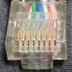
The plug is upside down; The clip is at the bottom.
Pin one is on the right hand side.
The wires connected to the even numbered contacts don't have any white.
Gigabit ethernet uses all 4 pairs;
| Pin | Signal | T568B Wire colour |
|---|---|---|
| 1 | A+ | White / Orange |
| 2 | A- | Orange |
| 3 | B+ | White / Green |
| 4 | C+ | Blue |
| 5 | C- | White / Blue |
| 6 | B- | Green |
| 7 | D+ | White / Brown |
| 8 | D- | Brown |
All pairs are bidirectional.
 -----+ +--------------- 4, 1 Or both
      | |
      ) (
      ) (
      ) *-- + PWR
      ) (
      ) (
      | |
 -----+ +--------------- 5, 2 Or both

 -----+ +--------------- 7, 3 Or both
      | |
      ) (
      ) (
      ) *-- - PWR
      ) (
      ) (
      | |
 -----+ +--------------- 8, 6 Or both
| Pin | T568A | T568B | 10/100 B | 10/100 A | Gigabit B | Gigabit A | ||||
|---|---|---|---|---|---|---|---|---|---|---|
| Colour | Colour | Signal | Power | Signal | Power | Signal | Power | Signal | Power | |
| 1 | Wt/Grn | Wt/Org | Rx+ | Rx+ | DC+ | A+ | A+ | DC+ | ||
| 2 | Green | Orange | Rx- | Rx- | DC+ | A- | A- | DC+ | ||
| 3 | Wt/Org | Wt/Grn | Tx+ | Tx+ | DC- | B+ | B+ | DC- | ||
| 4 | Blue | Blue | DC+ | C+ | DC+ | C+ | ||||
| 5 | Wt/Bl | Wt/Bl | DC+ | C- | DC+ | C- | ||||
| 6 | Orange | Green | Tx- | Tx- | DC- | B- | B- | DC- | ||
| 7 | Wt/Brn | Wt/Brn | DC- | D+ | DC- | D+ | ||||
| 8 | Brown | Brown | DC- | D- | DC- | D- | ||||
Using cross cables may reverse the polarity of the power.
Cat5e can be used up to 2.5 Gbps. Cat6a can be used up to 10 Gbps.
See: Twisted pair
Please note that some connectors are only suitable for stranded wire and
won't take solid core. Always check!
Solid is sometimes referred to as rigid and stranded as flexible.
In German stranded is called 'litze'.
For types of shielding, see:
Common
industry nomenclature for cable construction types.
I use solid core foil shielded (F/UTP) cat5e with T568B wiring at my place.
For new installations I would use S/FTP- or SF/FTP cat6a.
        1 2 3 4 5 6 7 8
    -----------------------
     \  * * * * * * * *  /
       \ * * * * * * * /
         -------------
           1
         9 0 1 2 3 4 5

              DA-15
 1    Shield
 2    Transmit (A)
 3    Control (A)
 4    Receive (A)
 5    Indication (A)
 6    Signal Timing (A)
 7    Byte Timing (A) (optional)
 8    Gnd

 9    Transmit (B)
10    Control (B)
11    Receive (B)
12    Indication (B)
13    Signal Timing (B)
14    Byte Timing (B) (optional)
15